Through-Hole Boards
Double-Sided Boards
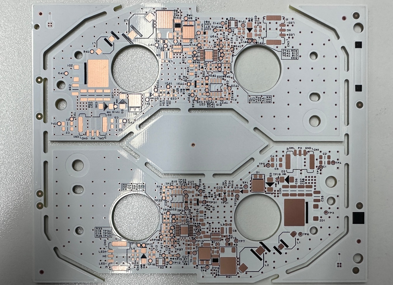
A double-sided PCB is a type of normal printing circuit board that has conductive layers on both sides. This means that both the top and bottom surfaces of the double-sided board can be used for the connection and installation of electronic components. It consists of a layer of substrate (usually using glass cloth) and two layers of copper foil, with the copper foil patterns etched out to form conductors, pads, and other necessary circuits.
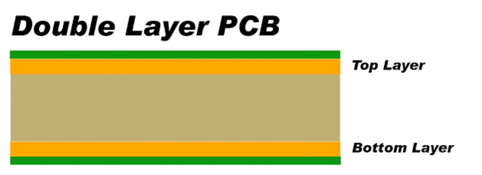
On a double-sided PCB, the connection between the top and bottom layers is achieved through via holes (small holes that connect the two copper layers) and plated-through holes (by adding copper plating conductive in the via holes). This allows for more complex circuit layouts and connections on a double-sided board, providing greater design flexibility.
Double-sided panels are commonly used in moderately designed electronic products, such as consumer electronics, power supply, and industrial control systems. Compared to multilayer boards, these panels offer higher circuit density and better signal integrity at a relatively lower cost.
Production Capacity
| Number of Layers | 2 layers |
| Board Thickness | 0.1mm-10mm |
| Maximum Copper Thickness | Outer layer 12oz |
| Minimum Line Width/Spacing | 0.038mm |
| Minimum Hole Dimension Tolerance | PTH ±0.05mm / NPTH ±0.05mm |
| Minimum Drilling Hole size | Mechanical drilling 0.15mm |
| Surface Treatment | OSP, Lead-free HASL, Immersion Gold, Gold Plating, Gold Fingers, Immersion Silver, Immersion Tin, Nickel-Palladium-Gold, Carbon Printing |
| Special Techniques | Resin plug hole + Electroplated cap (VIPPO), COIN/Embedded copper block technology, Edge plating, Press-fit, Controlled depth drilling/Routing, Semi-Flex, Back drilling |
Through-Hole Boards
Multilayer PCB
It is a type of normal printing circuit board composed of three or more layers, each with a conductive layer in the middle, using electrolytic copper foil or film layers to provide conductivity.
The structure of multilayer boards typically includes inner layers, outer layers, and interlayer connections. The inner layers are conductive layers located inside the board, made of copper foil or film materials. The outer layers are conductive layers located on the surface of the board, also made of copper foil or film materials. Interlayer connections are made through via holes (small holes that connect different layers), with copper plating conductive added to the via holes to achieve circuit connections.
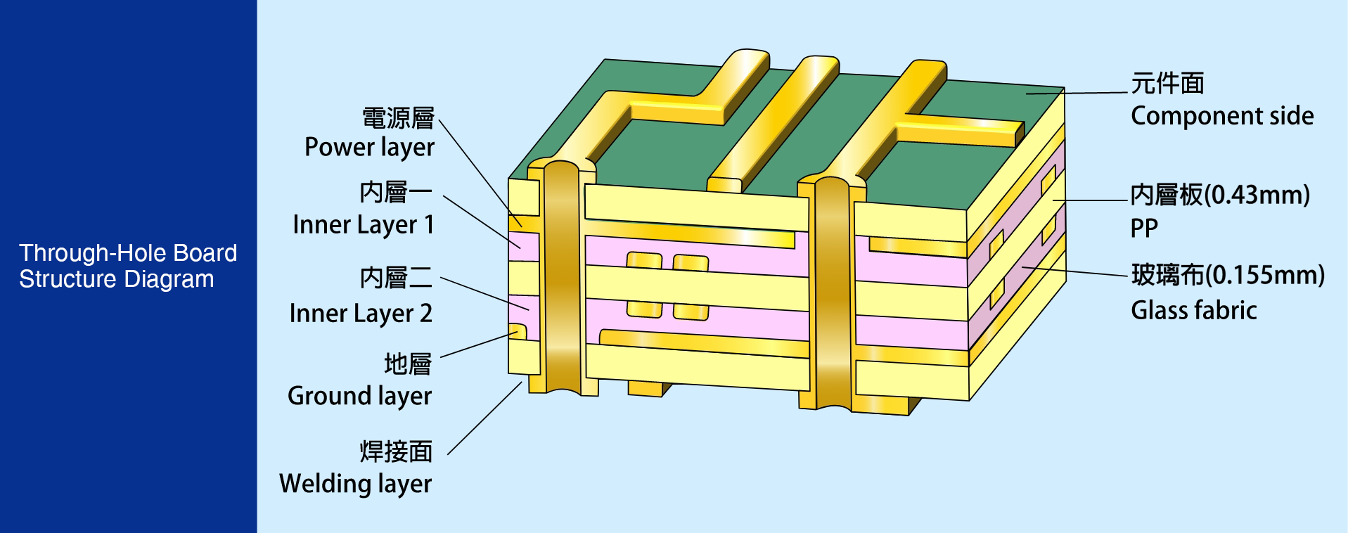
Multilayer boards provide higher circuit density and better signal integrity compared to single-sided and double-sided boards. They are commonly used in highly complex electronic products such as computers, communication network, medical equipment, and industrial control systems. Multilayer boards also offer better electromagnetic compatibility (EMC) and thermal performance, and can reduce the complexity of circuit routing.
Manufacturing multilayer boards requires more process steps and technology, making them more expensive to produce compared to single-sided and double-sided boards. However, due to their design and performance advantages, multilayer boards are widely used in modern electronic design.
Production Capacity
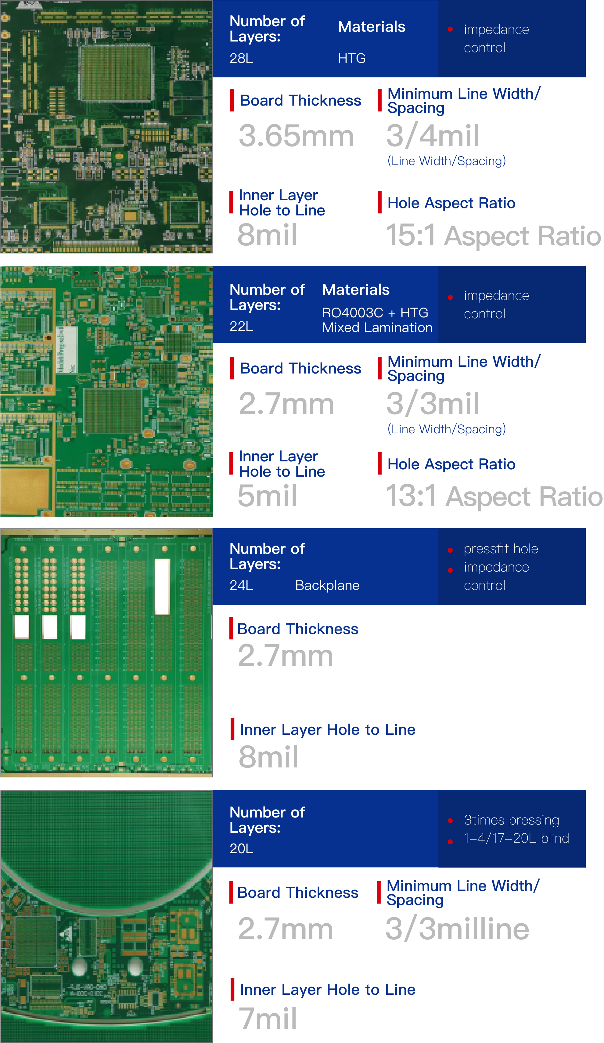
| Number of Layers | Single-sided to 50 layers |
| Board Thickness | 0.1mm-10mm, multilayer above 0.3mm |
| Maximum Copper Thickness | Inner Layer 10oz, Outer Layer 12oz |
| Minimum Line Width/Spacing | 0.038mm |
| Minimum Hole Dimension Tolerance | PTH ±0.05mm / NPTH ±0.05mm |
| Minimum Drilling Hole size | Mechanical Drilling 0.15mm, Laser Drilling 0.1mm |
| Surface Treatment | OSP, Lead-free HASL, Immersion Gold, Gold Plating, Gold Fingers, Immersion Silver, Immersion Tin, Nickel-Palladium-Gold, Carbon Printing |
| Special Techniques | Resin plug hole + Electroplated cap (VIPPO), COIN/Embedded copper block technology, Edge plating, Press-fit, Controlled depth drilling/Routing, Semi-Flex, Back drilling, Unbalanced Structure |
Through-Hole Boards
Heavy Copper PCBs
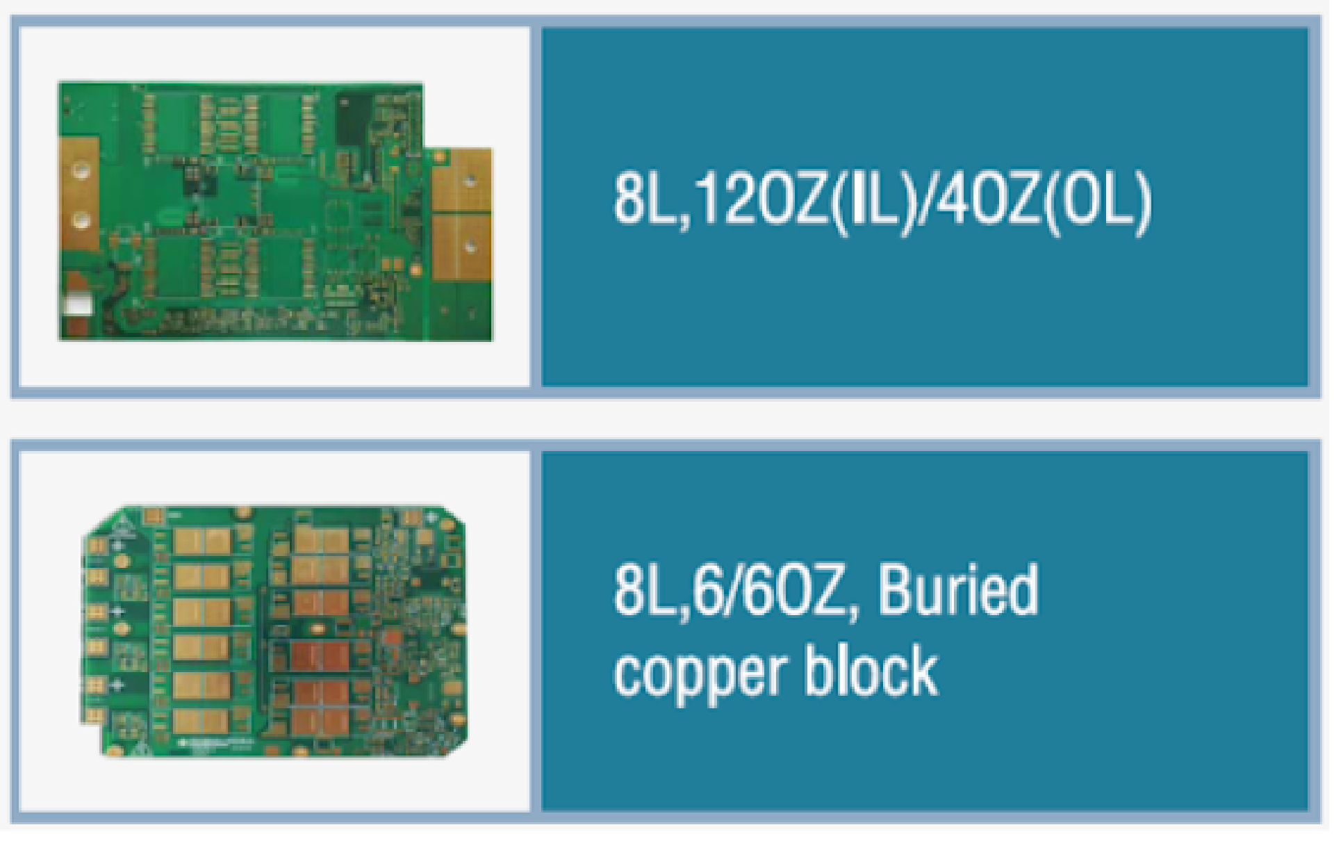
A type of printing circuit board with a thicker copper foil than traditional PCBs. Typically, a standard PCB's copper foil layer thickness ranges from 1 oz to 3 oz, while the copper foil thickness of heavy copper PCBs usually exceeds 3 oz.
| The main features of heavy copper PCBs are as follows: |
| Current Conductivity: Due to the increased thickness of the copper foil layer, heavy copper PCBs can provide higher current conductivity. This makes them particularly suitable for high-power and high-current applications, such as power electronics, power tools, and industrial equipment. |
| Thermal Conductivity: Due to the excellent thermal conductivity of copper, heavy copper PCBs can effectively dissipate heat across the entire board. By improving heat dissipation, this makes heavy copper PCBs very useful in applications requiring good thermal performance, such as LED lighting products and electronic heat sinks. |
| Mechanical Strength: Due to the increased thickness of the copper foil, heavy copper PCBs have higher mechanical strength and durability compared to standard PCBs. This allows them to withstand greater physical stress and vibration while providing better structural support. |
| Soldering Performance: Due to the increased thickness of the copper foil, heavy copper PCBs can provide better soldering contact and thermal conductivity during the soldering process. This makes the soldering process more reliable and easier to handle. |
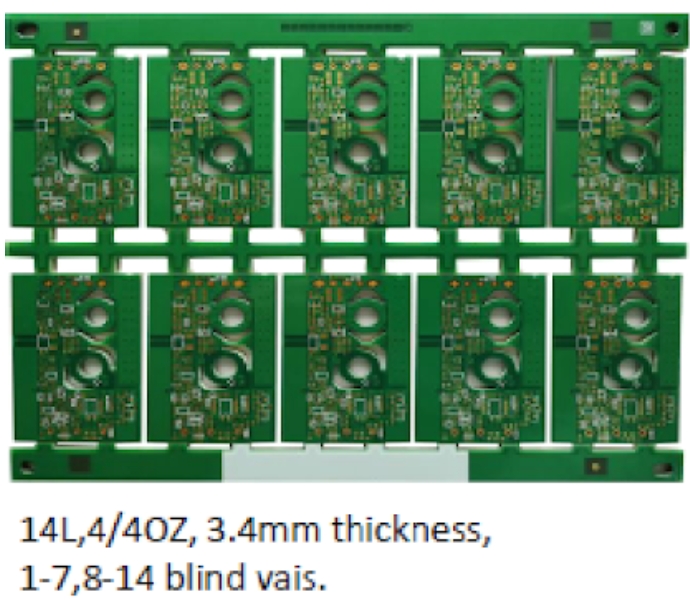
Heavy copper PCBs are typically used in application that demand high current conductivity, good thermal performance, and mechanical strength. They are widely used in power supplies, industrial control systems, automotive electronics and solar systems. However, due to their special manufacturing process and higher costs, heavy copper PCBs may require longer production cycles and higher costs compared to standard PCBs.
Production Capacity
| Number of Layers | Single-sided to 50 layers |
| Board Thickness | 0.1mm-10mm, multilayer above 0.3mm |
| Maximum Copper Thickness | Inner Layer 10 oz, Outer Layer 12 oz |
| Minimum Line Width/Spacing | 0.038mm |
| Minimum Hole Dimension Tolerance | PTH ±0.05mm / NPTH ±0.05mm |
| Minimum Drilling Hole size | Mechanical Drilling 0.15mm, Laser Drilling 0.1mm |
| Surface Treatment | OSP, Lead-free HASL, Immersion Gold, Gold Plating, Gold Fingers, Immersion Silver, Immersion Tin, Nickel-Palladium-Gold, Carbon Printing |
| Special Techniques | Resin plug hole + Electroplated cap (VIPPO), COIN/Embedded copper block technology, Edge plating, Press-fit, Controlled depth drilling/Routing, Semi-Flex, Back drilling, Unbalanced Structure |
Through-Hole Boards
High-Frequency Circuit Boards (RF – Radio Frequency)
A type of printing circuit board designed for wireless communication and high-frequency applications. High-frequency circuit boards are typically used to handle and transmit RF signals, characterized by excellent high-frequency performance and signal integrity.
| RF circuit boards need to consider several special factors to ensure their proper operation, including: |
| High-frequency signal characteristics: RF circuit boards require low transmission loss, minimal interference, and reduced noise for high-quality signal transmission. |
| High-frequency design and routing: The design of RF circuit boards needs to consider the propagation and matching of RF signals to minimize signal attenuation and reflection. |
| Good ground plane and shielding: To reduce interference and crosstalk, RF circuit boards typically require proper ground planes and shielding structures. |
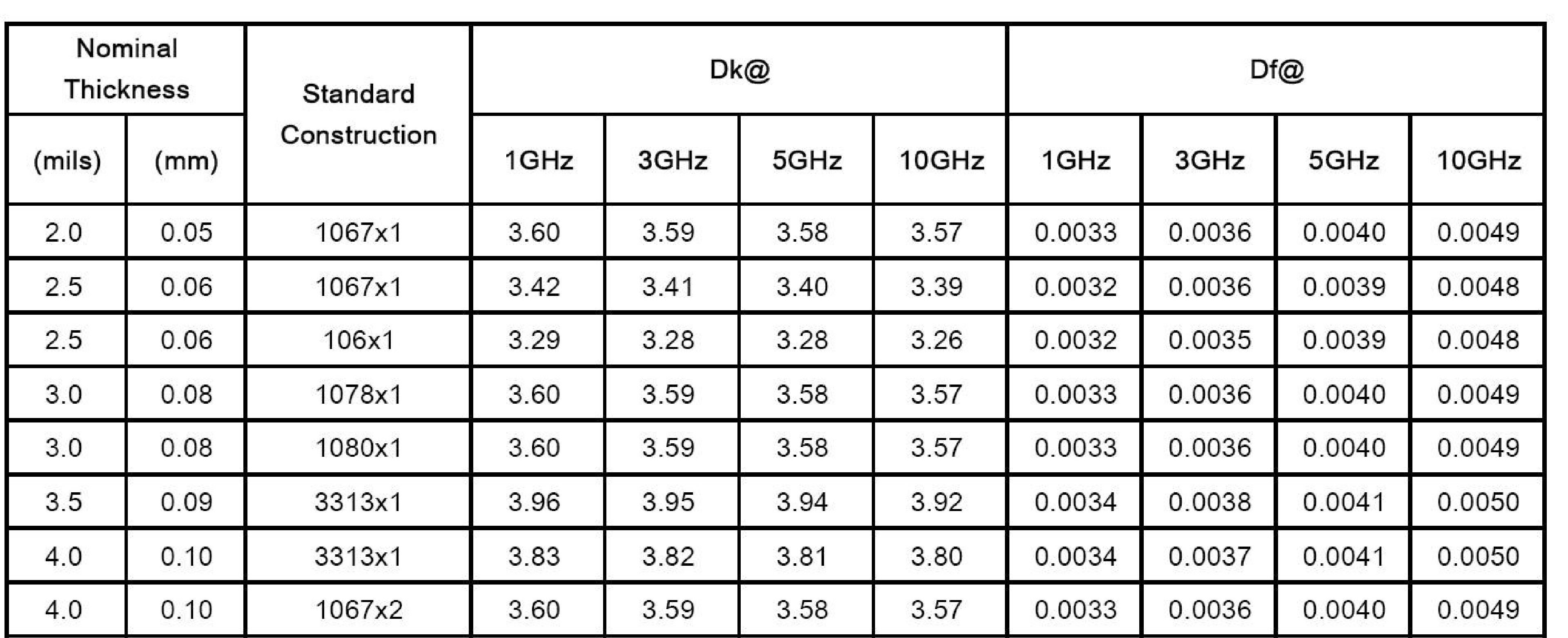
| High-frequency materials: Choosing appropriate high-frequency materials is crucial. These materials have lower dielectric loss and higher conductivity to ensure signal stability and consistency. |

RF circuit boards are widely used in high-frequency applications such as wireless communication systems, satellite communications, radar systems, and wireless sensor networks. They are used to transmit and process RF signals, ensuring high-quality and stable signals for reliable wireless communication and high-frequency applications.
Production Capacity
| Number of Layers | Single-sided to 50 layers |
| Board Thickness | 0.1mm-10mm, multilayer above 0.3mm |
| Maximum Copper Thickness | Inner Layer 10 oz, Outer Layer 12 oz |
| Minimum Line Width/Spacing | 0.038mm |
| Minimum Hole Dimension Tolerance | PTH ±0.05mm / NPTH ±0.05mm |
| Minimum Drilling Hole size | Mechanical Drilling 0.15mm, Laser Drilling 0.1mm |
| Surface Treatment | OSP, Lead-free HASL, Immersion Gold, Gold Plating, Gold Fingers, Immersion Silver, Immersion Tin, Nickel-Palladium-Gold, Carbon Printing |
| Special Techniques | Resin plug hole + Electroplated cap (VIPPO), COIN/Embedded copper block technology, Edge plating, Press-fit, Controlled depth drilling/Routing, Semi-Flex, Back drilling, Unbalanced Structure |
Through-Hole Boards
Semi-Flex PCB
A Semi-Flex PCB is a particular type of printing circuit board that combines the characteristics of both flexible and rigid boards. It has bending capabilities that lie between those of rigid and fully flexible boards.
| The main features of Semi-Flex PCBs are as follows: |
| Flexibility: Semi-Flex PCBs have a certain degree of bending ability, but the bending area is relatively limited compared to fully flexible boards. This allows Semi-Flex PCBs to adapt to specific shape and size requirements while providing greater structural stability. |
| Rigid Areas: Semi-flex PCBs typically include rigid areas made of hardboard materials (such as FR4), which provide structural support and protect larger and more complex electronic components. |
| Flexible connections: Semi-flex PCBs utilize flexible connection layers to link rigid and flexible areas. These connection layers typically comprise flexible copper foil or flexible materials (such as polyimide), providing strong elasticity and conductivity for dependable electrical connections and signal transmission. |

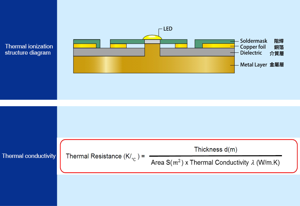
Semi-Flex PCBs are commonly used in scenarios that require a combination of rigidity and flexibility, such as automotive electronics, medical devices, and aerospace applications. They offer flexible design options while maintaining a certain degree of structural stability. However, due to the complexity of their design and manufacturing, specialized processes and technologies are required to ensure the reliability and performance of the product.
Production Capacity
| Number of Layers | Single-sided to 50 layers |
| Board Thickness | 0.1mm-10mm, multilayer above 0.3mm |
| Maximum Copper Thickness | Inner Layer 10 oz, Outer Layer 12 oz |
| Minimum Line Width/Spacing | 0.038mm |
| Minimum Hole Dimension Tolerance | PTH ±0.05mm / NPTH ±0.05mm |
| Minimum Drilling Hole size | Mechanical Drilling 0.15mm, Laser Drilling 0.1mm |
| Surface Treatment | OSP, Lead-free HASL, Immersion Gold, Gold Plating, Gold Fingers, Immersion Silver, Immersion Tin, Nickel-Palladium-Gold, Carbon Printing |
| Special Techniques | Resin plug hole + Electroplated cap (VIPPO), COIN/Embedded copper block technology, Edge plating, Press-fit, Controlled depth drilling/Routing, Semi-Flex, Back drilling, Unbalanced Structure |
HDI (High-Density Interconnect)
HDI(High-Density Interconnect)
HDI is a high-density interconnect technology used to manufacture printing circuit boards. HDI technology aims to achieve higher circuit density and more complex electronic component connections to meet the demands of modern electronic products, which are becoming smaller in size and higher in functionality. HDI PCBs feature multiple levels of interconnections, including inner layer connections, through-holes, and microvias.
| Characteristics of HDI PCBs include: |
| Higher layer count: HDI PCBs typically have a multilayer structure, allowing for more circuit layers in a smaller space. |
| Smaller through-holes and microvias: The size of through-holes and microvias is smaller, saving valuable board space. |
| Higher circuit density: HDI PCBs can achieve higher circuit density, allowing more signal and power channels to pass through limited space. |
| Shorter signal transmission distance: Due to the high-density characteristics of HDI PCBs, the signal transmission distance is relatively short, reducing the risk of signal attenuation and interference. |
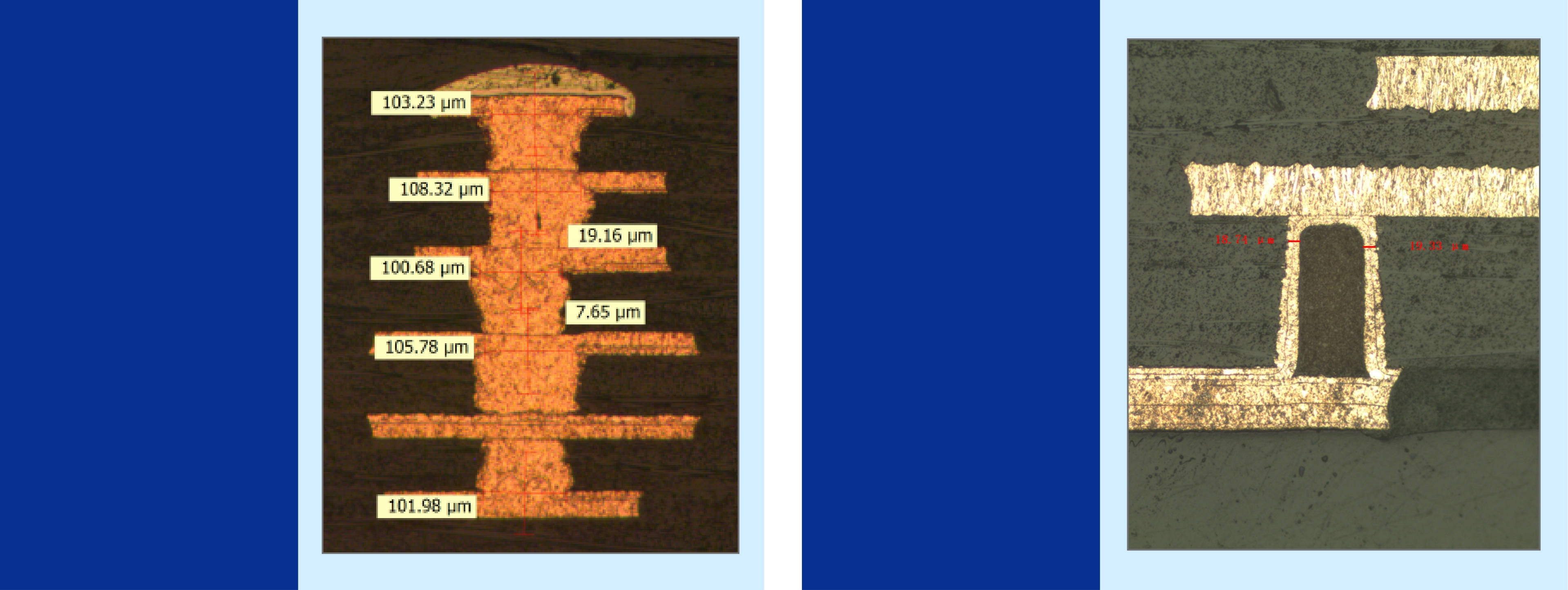
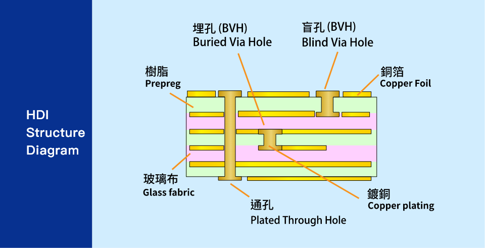
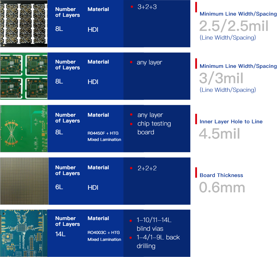
Anylayer is an advanced HDI technology that allows for a greater number of layers and higher circuit density on a printing circuit board. Anylayer typically uses smaller through-holes and microvias to achieve more complex electronic component connections.
HDI technology is widely used in many applications, especially in smartphones, tablets, digital cameras, and other small portable devices. It provides smaller, lighter, and higher-performance solutions while offering greater flexibility and feasibility for complex electronic designs.
Production Capacity
| Number of Layers | 18L any layer interconnect |
| Board Thickness | 0.1mm-10mm, multilayer above 0.3mm |
| Maximum Copper Thickness | Inner layer 1oz, outer layer Toz |
| Minimum Line Width/Spacing | 0.038mm |
| Minimum Hole Dimension Tolerance | PTH ±0.05mm / NPTH ±0.05mm |
| Minimum Drilling Hole size | Mechanical drilling 0.15mm, laser drilling 0.1mm |
| Surface Treatment | OSP, Lead-free HASL, Immersion Gold, Gold Plating, Gold Fingers, Immersion Silver, Immersion Tin, Nickel-Palladium-Gold, Carbon Printing |
Insulated Metal Substrate (IMS)
Insulated Metal Substrate (IMS)
IMS (Insulated Metal Substrate) is a type of insulated metal substrate technology commonly used in high-power electronic devices and thermal management applications. IMS substrates combine the characteristics of metal substrates and insulation layers, providing excellent thermal performance and circuit isolation.
| The structure of IMS substrates typically includes three main parts: |
| Metal substrate: The base layer of an IMS substrate is a metal material, usually aluminum or copper. The metal substrate has good thermal performance, allowing it to quickly transfer heat to the surrounding environment. |
| Insulation layer: Above the metal substrate, there is an insulation layer (usually ceramic or organic material) used to isolate the circuit layer from the metal substrate, preventing short circuits and interference. |
| Circuit layer: On top of the insulation layer, there is one or more circuit layers used for the connection and assembly of electronic components. |

| The main advantages of IMS substrates include: |
| Thermal performance: The excellent thermal characteristics of metal substrates can effectively transfer and dissipate heat, improving the efficiency and reliability of electronic components. |
| High-power applications: IMS substrates are suitable for high-power electronic devices, such as high-power LED lighting, power modules, and power electronics. |
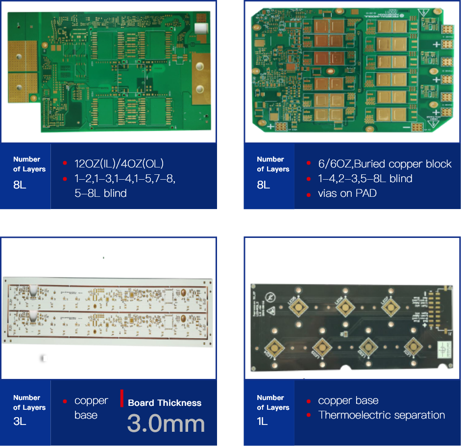
IMS substrates are widely used in various fields, including lighting, automotive electronics, industrial electronics, communications, and energy, to provide thermal solutions and circuit isolation for high-power applications.
Production Capacity
| Number of Layers | Single-sided to 8 layers |
| Materials | Aluminum-based, Copper-based, Iron-based, Mirror aluminum |
| Board Thickness | 0.4mm-3.2mm |
| Maximum Copper Thickness | Inner layer 2oz, outer layer 4oz |
| Minimum Line Width/Spacing | 0.10mm |
| Minimum Hole Dimension Tolerance | PTH ±0.075mm / NPTH ±0.05mm |
| Minimum Drilling Hole size | Mechanical drilling 0.15mm, laser drilling 0.1mm |
| Surface Treatment | OSP, Lead-free HASL, Immersion Gold, Immersion Silver, Immersion Tin, Nickel-Palladium-Gold, Carbon Printing |
| Thermal conductivity | 12W, single-sided aluminum-based |
| Special Techniques | DVCP, Thermal and electrical separation, High reflectivity mirror |
Rigid-Flex PCB
Rigid-Flex PCB
A Rigid-Flex PCB is a special type of printing circuit board that combines rigid and flexible areas, connected together by flexible connection layers. This structure allows the PCB to have the characteristics of both rigid and flexible boards.
| The main features of Rigid-Flex PCBs are as follows: |
| Rigid Areas: Rigid areas are usually made of hardboard materials (such as FR4), offering superior structural stability and robustness, capable of accommodating larger and more complex electronic components. |
| Flexible Areas: Flexible areas are made of flexible materials (such as polyimide), allowing for bending, folding, and free variation in bending dimensions. This enables Rigid-Flex PCBs to accommodate space constraints with special shapes or flexible design requirements. |
| Flexible Connection Layers: The rigid and flexible areas of Rigid-Flex PCBs are connected using flexible connection layers. These layers are typically made of flexible copper foil or polyimide film, providing reliable electrical connections and signal transmission. |
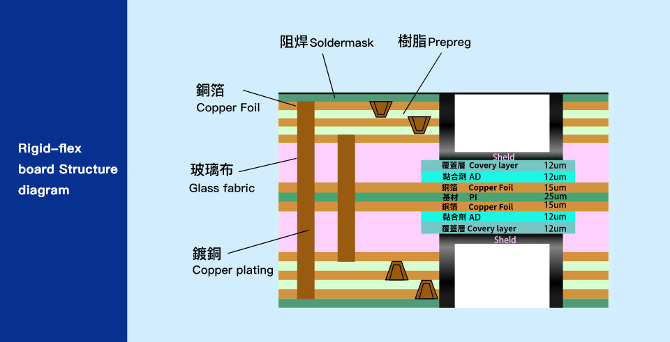
Rigid-Flex PCBs are very useful in applications that require both rigidity and flexibility. Due to their excellent functionality and reliability, they are used in wearable devices, foldable phones, military, and aerospace systems. The design and manufacturing of Rigid-Flex PCBs are relatively complex, requiring special processes and technologies, but they offer more flexible, space-saving, and reliable solutions to meet diverse application needs.
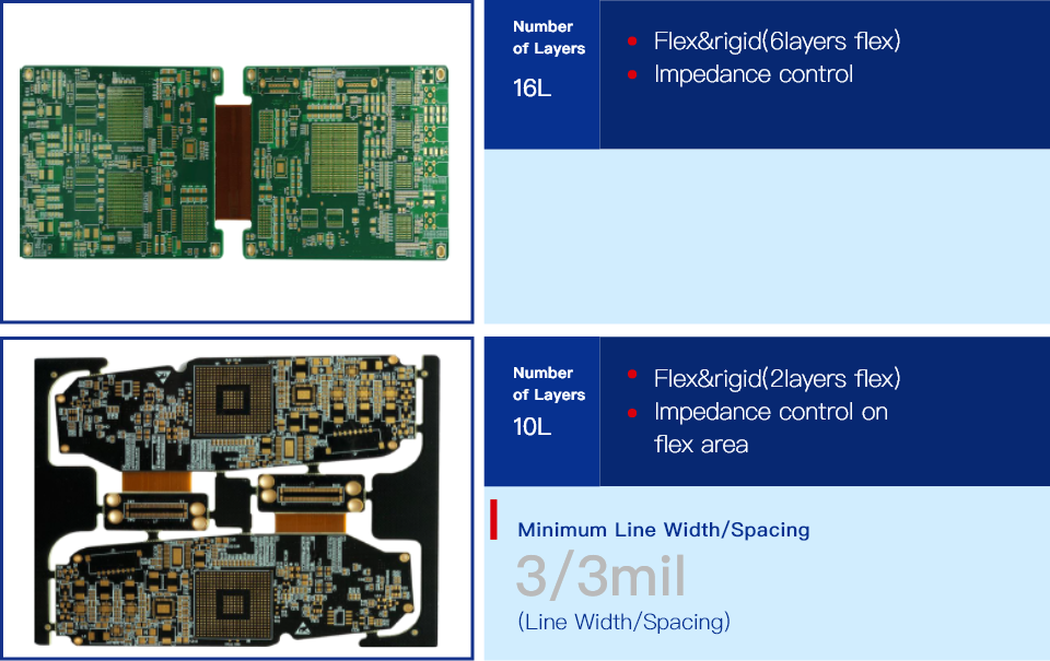
Production capacity (hard board part)
| Number of Layers | 4 layers to 24 layers |
| Board Thickness | 0.1mm-10mm, multilayer above 0.3mm |
| Maximum Copper Thickness | Inner layer 8 oz, outer layer 12 oz |
| Minimum Line Width/Spacing | 0.035mm |
| Minimum Hole Dimension Tolerance | PTH ±0.05mm / NPTH ±0.05mm |
| Minimum Drilling Hole size | Mechanical drilling 0.15mm, laser drilling 0.1mm |
| Surface Treatment | OSP, Lead-free HASL, Immersion Gold, Gold Plating, Gold Fingers, Immersion Silver, Immersion Tin, Nickel-Palladium-Gold, Carbon Printing |
| Special Techniques | Resin plug hole + Electroplated cap (VIPPO), COIN/Embedded copper block technology, Edge plating, Press-fit, Controlled depth drilling/Routing, Back drilling |
Production capacity (soft board part)
| Number of Layers | Single-sided to 12 layers |
| Board Thickness | Minimum 0.05mm finished |
| Minimum Line Width/Spacing | 0.035mm |
| Minimum Hole Dimension Tolerance | PTH ±0.05mm / NPTH ±0.05mm |
| Minimum Drilling Hole size | Mechanical drilling 0.15mm, laser drilling 0.1mm |
| Surface Treatment | OSP, Immersion Gold, Gold Plating |
| Rigid-flex capability | YES |
| Special Techniques | Air-Gap,Bonding,Fly-tail,Unsymmetrical,Semi-flex |
Flexible circuit board (Flexible PCB)
Flexible circuit board (Flexible PCB)
A printing circuit board with bending and folding capabilities. Unlike traditional rigid boards, flexible circuit boards use flexible substrates, such as polyimide (PI), to achieve bending and folding.
| Flexible Printing Circuit Boards (FPC): |
| Flexibility: FPC can be bent without damage or loss of function, adapting to different shape and size requirements. |
| Thin and light: FPC are thinner and lighter than traditional rigid boards, making them more advantageous in applications with size and weight constraints. |
| High density: Due to the flexibility of FPC, they can achieve higher circuit density and smaller packaging, providing more functionality and design flexibility. |
| Reliability: FPC have excellent stress resistance and fatigue resistance, maintaining stable electrical performance during long-term use and bending. |
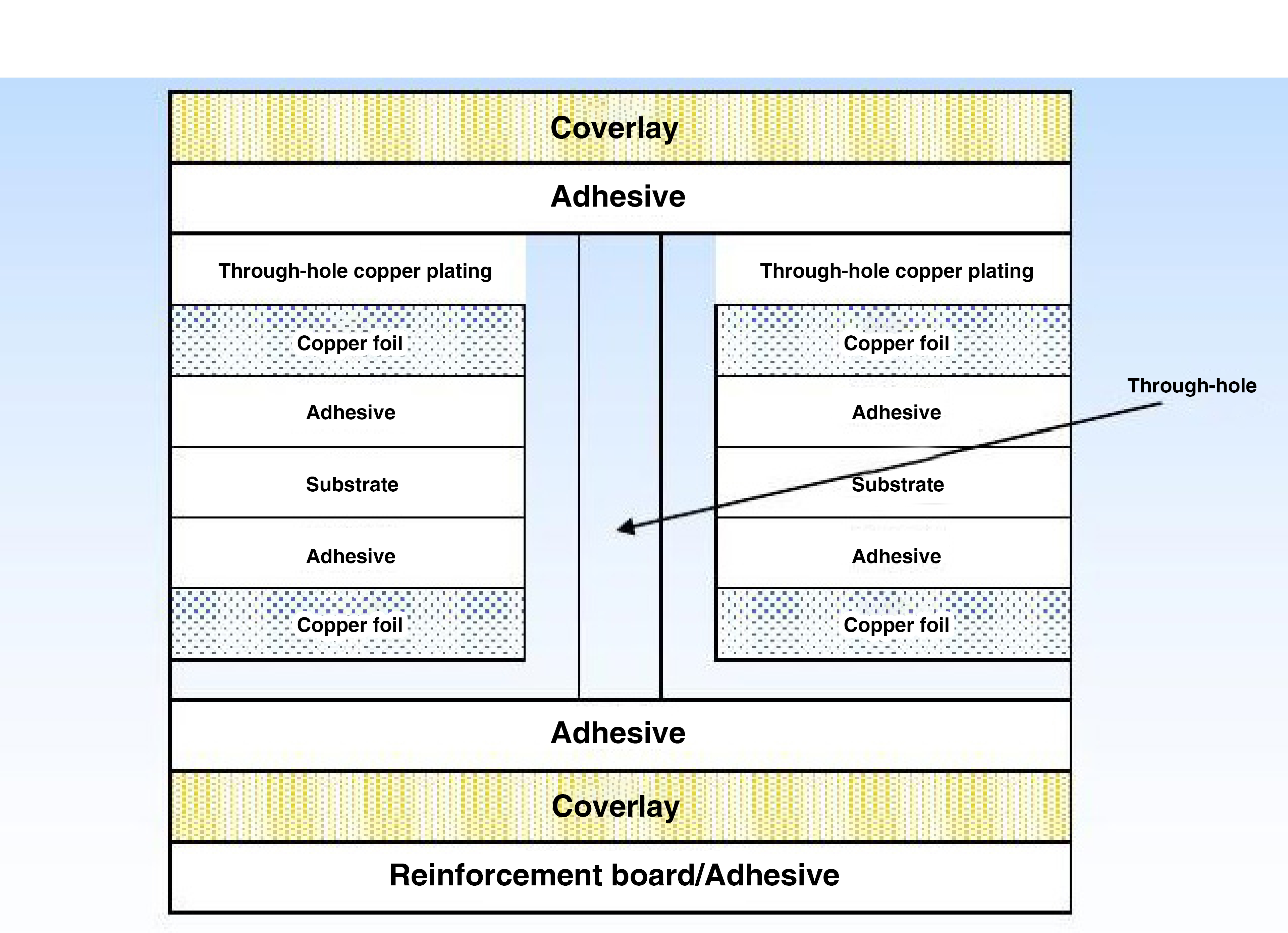
FPC are widely used in many applications, especially in scenarios requiring bending or limited space. For example, mobile devices, wearable devices, foldable displays, automotive electronics, medical devices, etc. They provide more flexible, reliable, and lightweight solutions while meeting the requirements of modern electronic designs.
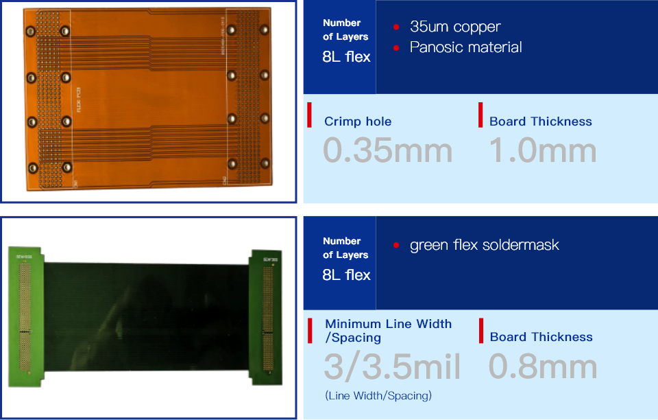
Production capacity (soft board part)
| Number of Layers | Single-sided to 12 layers |
| Board Thickness | Minimum 0.05mm finished |
| Minimum Line Width/Spacing | 0.035mm |
| Minimum Hole Dimension Tolerance | PTH ±0.05mm / NPTH ±0.05mm |
| Minimum Drilling Hole size | Mechanical drilling 0.15mm, laser drilling 0.05mm |
| Surface Treatment | OSP, Immersion Gold, Gold Plating |
| Rigid-flex capability | YES |
| Special Techniques | Air-Gap,Bonding,Fly-tail,Unsymmetrical,Semi-flex |
